Hi-Tech Products Die Cutting and Converting

Microfluidics

Microfluidics Device Manufacturing

Microfuidic Device Components

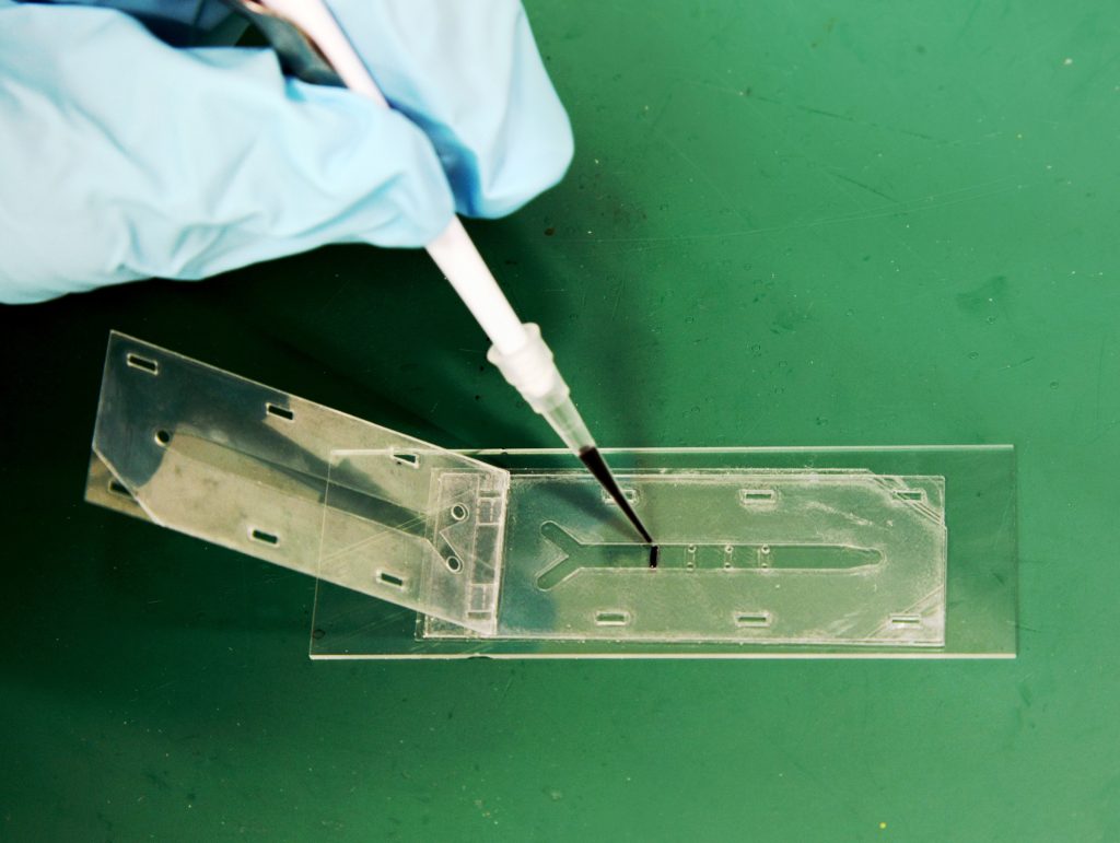
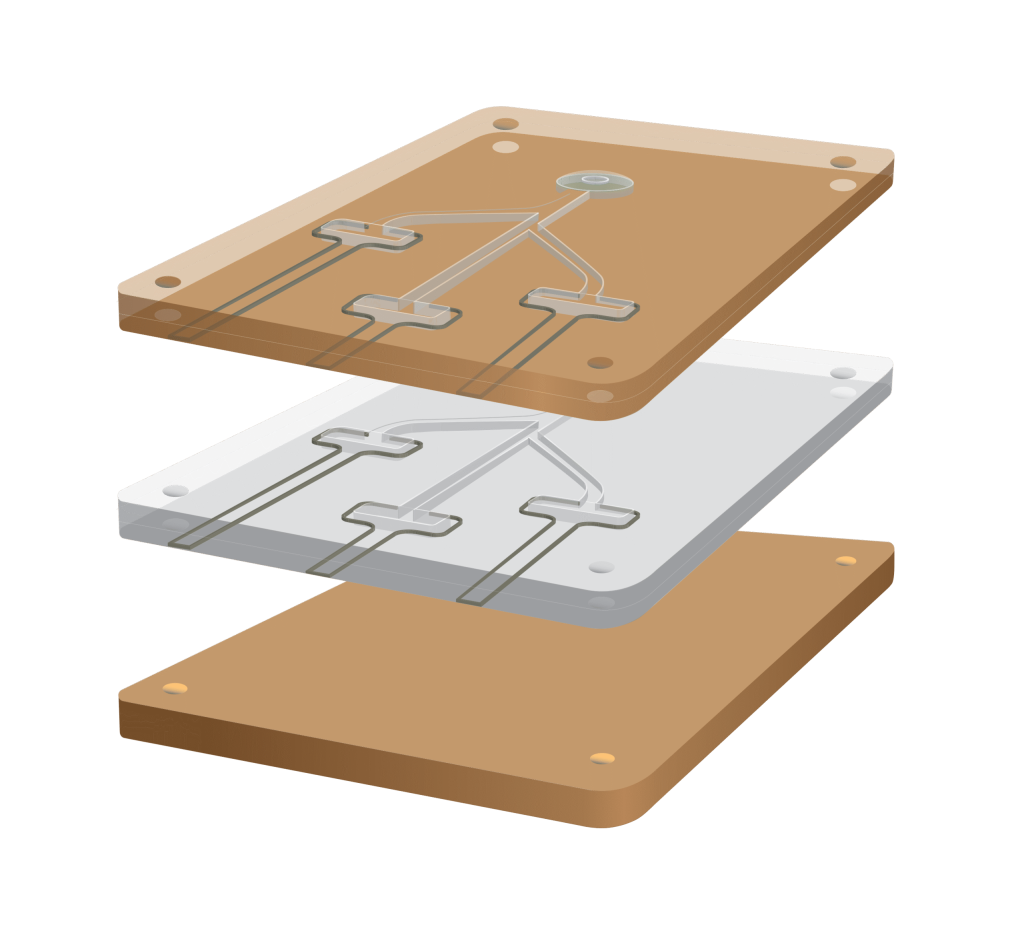
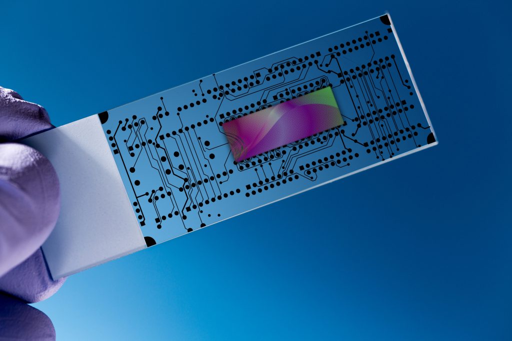
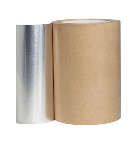
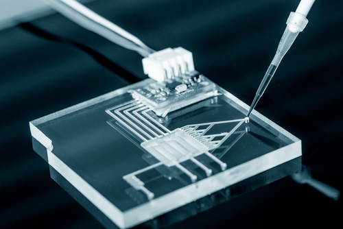
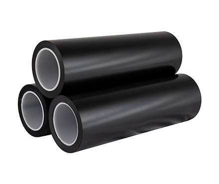
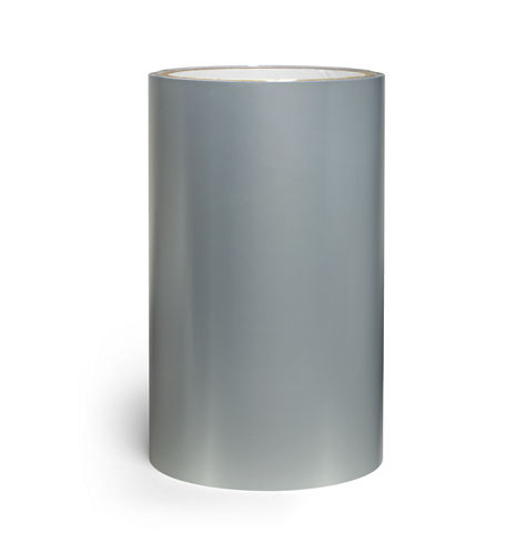
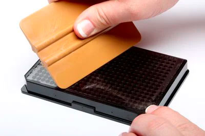
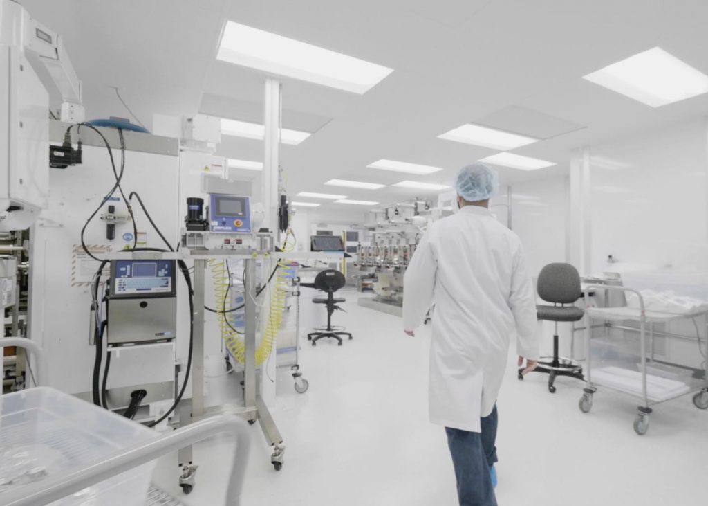
Our ISO certified facilities and expertise are well suited for manufacturing: microfluidic chips, flow cells, PCR chips, cartridge consumables, lateral-flow, NGS flow cells, and wearable patches. Hi-Tech Products can provide the materials and converting processes necessary to manufacture your microfluidic device components. Materials may include converted film, membrane, and foil components commonly found in microfluidic device assemblies.

Structural & optical films

  • Optical cover / detection window
    • Materials: COC, COP, PC, PMMA, thin glass.
    • Thickness: 50–1000 µm (commonly 100–500 µm).
    • Processes: laser cutting, die-cutting, precision sheeting, ultrasonic welding prep.
    • Use: fluorescence/absorbance readout, microscope optics, alignment windows.
  • Substrate film (bulk structural layer)
    • Materials: COC/COP, PC, PET, PEN.
    • Thickness: 100–2000 µm.
    • Processes: die-cutting, CNC routing (if laminated to rigid support).
    • Use: base layer for channels, mounting reagents, mechanical support.

Adhesive & bonding layers

  • Pressure-sensitive adhesive (PSA) die-cuts / transfer tapes
    • Materials: acrylic PSAs, silicone PSAs, rubber PSAs (medical grade).
    • Thickness: 25–250 µm (1–10 mil).
    • Processes: lamination, kiss-cut, through-cut, transfer coating.
    • Use: seal microfluidic layers, form channels by selective bonding, tack for assembly.
  • Thermoplastic welding films / thermal bond adhesives
    • Materials: polyethylene, polypropylene, specialized thermoplastic films.
    • Thickness: 25–200 µm.
    • Processes: thermal lamination, impulse welding.
    • Use: permanent seals for reaction chambers that require high-temp exposure.
  • Double-sided tape with patterned release liners
    • Use: rapid assembly, pre-registered adhesive patterns to control fluid paths.

Channel-defining & spacer films

  • Patterned spacer adhesives (channel-forming die-cuts)
    • Materials: acrylic adhesive on PET/film carriers, laser-cut PSA.
    • Thickness: 25–500 µm depending on channel depth.
    • Processes: die-cut, laser-cut, plotter cutting.
    • Use: define channel geometry, create reaction chamber volumes.
  • Embossable thermoplastic films for molded channels
    • Materials: COC, COP, PC.
    • Processes: embossing, hot-emboss die forming.
    • Use: formed microchannels for precise fluid handling.

Membranes for filtration, venting, and metering

  • Hydrophobic vent membranes (air venting / bubble trap)
    • Materials: PTFE, ePTFE, PVDF with hydrophobic treatment.
    • Pore sizes: 0.1–5 µm (application dependent).
    • Processes: die-cut, adhesive-backed options.
    • Use: allow air escape while blocking liquid; pressure relief vents.
  • Hydrophilic membranes (wicking / flow control / capillary stop)
    • Materials: nitrocellulose (lateral flow), cellulose, polyethersulfone (PES), hydrophilized PTFE.
    • Pore sizes: 0.1–10 µm.
    • Processes: precision die-cutting, overlamination.
    • Use: capillary flow, reagent distribution, filtration.
  • Filtration membranes (particle/virus filtering)
    • Materials: PES, PVDF, cellulose acetate, nylon.
    • Pore sizes: 0.02–5 µm.
    • Use: remove particulates, pre-filter sample.
  • Porous foam membranes (wicking / absorbent pads)
    • Materials: PU foam, cellulose foam.
    • Use: waste reservoirs, absorb excess reagent.

Valve, burst, and metering films

  • Pressure-actuated valve membranes
    • Materials: thin elastomers (TPU, PDMS), laminated films with cutouts.
    • Thickness: 25–200 µm.
    • Use: on-chip valves that open/close with pressure or vacuum.
  • Burstable foil / peel-seal membranes (reagent isolation)
    • Materials: aluminum foil laminates, metallized PET, multi-layer foil.
    • Processes: die-cut, heat-seal, laser scoring.
    • Use: isolate lyophilized reagents or reagents until use; scored weak points for controlled rupture.
  • Capillary burst valves (hydrophobic patches on film)
    • Materials: surface-treated PET/COC with hydrophobic coatings or patterned adhesives.
    • Use: passive flow control via capillary pressure thresholds.

Reagent & storage films / seals

  • Foil laminate seals (moisture/oxygen barrier)
    • Materials: Al foil laminated with PET/LDPE; multi-layer barrier films.
    • Processes: form-fill-seal, die-cut seals.
    • Use: reagent pouch covers, lyophilized reagent pouches, long-term storage.
  • Desiccant films / sachet foils
    • Materials: laminated foil pouches, breathable desiccant-embedded films.
    • Use: maintain dry environment for reagents.
  • Transfer/spotting carriers for dried reagents (paper/film backing)
    • Materials: glass fiber pads, porous membranes laminated to film.
    • Use: hold lyophilized enzymes, primers, probes inside chamber.

Conductive & thermal films

  • Printed conductive traces / thin-film heaters
    • Materials: silver/graphene/sputtered metal traces on polyimide, PET, or COC.
    • Processes: screen print, inkjet, sputter, flex circuit lamination.
    • Use: on-chip heaters for PCR thermal cycling, temperature sensors, electrical contacts.
  • Flexible printed circuit interposers (polyimide flex)
    • Materials: polyimide with copper traces, laminated to PET.
    • Use: connect chip electrodes to instrument, sense signals, apply voltage.
  • Thermal interface films / heat-spreading foils
    • Materials: graphite films, thin metal foils.
    • Use: even heat distribution across reaction chambers.

Optical control & stray-light management

  • Black/opaque films
    • Materials: black PET, black COC, carbon-loaded films.
    • Use: prevent optical cross-talk between wells and block stray light.
  • Reflective films / metallized foils
    • Materials: aluminized PET.
    • Use: increase signal by reflecting excitation/emission.
  • Anti-reflective / anti-glare coatings on detection windows
    • Processes: coatings applied to films for better optical performance.

Surface-treated films & coatings

  • Hydrophilic surface treatments (promote wetting)
    • Methods: plasma, corona, chemical grafting, surfactant coatings.
    • Use: control capillary flow, reduce air bubbles.
  • Hydrophobic coatings / patterning
    • Use: capillary stops, channel definition.
  • Anti-fouling / PEG coatings
    • Use: reduce nonspecific protein/DNA adsorption, improve assay sensitivity.
  • Adhesion promotion layers
    • Use: improve bonding between dissimilar plastics or adhesives.
corona treatment

Release liners & handling carriers

  • Silicone-coated release liners (paper or film-backed)
    • Use: protect PSA until assembly, register die-cuts for pick-and-place.
  • Low-tack carrier films (transfer tapes)
    • Use: temporary support of fragile microfluidic components during assembly.

Lidding & user interface films

  • Peelable user-access films
    • Materials: easy-peel laminates, scored foils with tamper-evident features.
    • Use: sample ports, user-accessible reagent chambers.
  • Labeled overlays / instruction films
    • Materials: printable PET/PVC overlays, with tactile features.
    • Use: labeling, user guidance, barcode placement.

Sterilization- & process-compatibility notes

  • Gamma / EtO / E-beam compatibility: specify material compatibility up front (e.g., some PSAs yellow or lose adhesion under gamma).
  • Autoclave: most polymer films warp; use only materials rated for steam if required.
  • Shelf-life & packaging: barrier foils + desiccants often required for lyophilized reagents.

Typical converting processes used

  • Die-cutting & kiss-cutting — precision cut shapes for PSAs, membranes.
  • Laser cutting — tight tolerances, small features, no tooling.
  • Lamination — roll-to-roll or sheet lamination to build stacks.
  • Embossing / hot-emboss — create microchannels in thermoplastics.
  • Printed electronics (screen/inkjet/sputter) — heaters, traces, electrodes.
  • Thermal/ultrasonic/laser welding — permanent seals between thermoplastic layers.
  • Plasma/corona treatment & coating — tuning surface energy.
  • Punching & stamping — high-volume shapes.
cleanroom converting and rotary die cutting

Typical tolerances & specs to call out on drawings

  • Channel depth tolerance: ±5–20 µm (depends on process).
  • Die-cut hole positional tolerance: ±0.05–0.25 mm (depending on tool & material).
  • Adhesive placement tolerance: ±0.2 mm typical for high-precision.
  • Surface roughness / optical clarity: specify % haze, transmission.
  • Pore size distribution (membranes): specify mean pore size ± SD.
  • Biocompatibility: USP Class VI / ISO 10993 requirements if in contact with sample or tissue.

Example component→material→use quick mapping (short)

  • PCR optical window → COC, 200 µm → fluorescence read.
  • Channel spacer → PSA on PET, 100 µm die-cut → microchannel definition.
  • Reagent foil seal → Al/PET/LDPE laminate → foil seal over reagent well.
  • Hydrophobic vent → ePTFE membrane, 0.2 µm → air vent.
  • Lyophilized reagent pad → glass-fiber pad laminated to substrate → dried enzyme spot.
  • On-chip heater → printed silver on polyimide → rapid thermal cycling.

Substrate & Cover Films – These form the top and bottom structural layers of the microfluidic device.

Polycarbonate (PC) 125-500 µm

  • Optically clear, rigid, low autofluorescence, good machinability.
  • Common in thermally bonded chips; stable for analytical or diagnostic use.

Cyclo Olefin Polymer (COP) / Cyclo Olefin Copolymer (COC) 100–500 µm

  • Exceptional optical clarity, low water absorption, excellent chemical resistance.
  • Gold standard for optical biosensors, DNA analysis, and diagnostic cartridges.